 This time, I have a true curiosity for you. 🙂
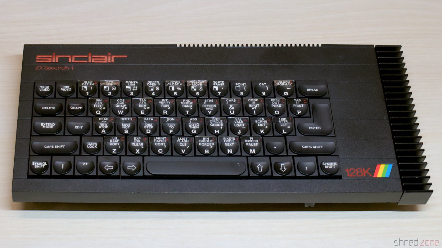
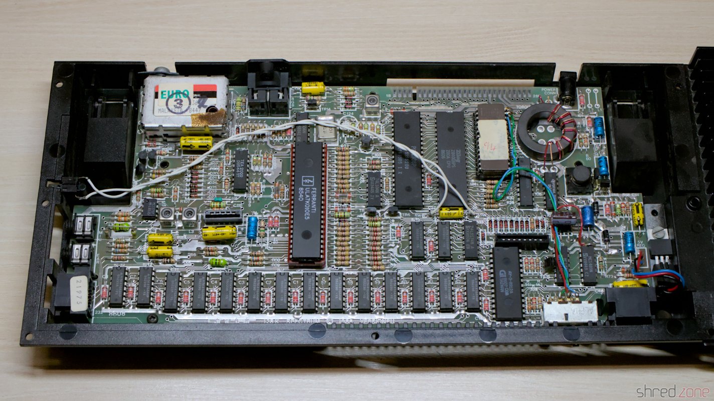
It's a ZX Spectrum 128K. It was designed by Sinclair and their Spanish distributor Investrónica, and was a major upgrade of the ZX Spectrum 48K. At that time, the 48K model was rather outdated with its limited RAM and the simple sound beeper, and Sinclair had nothing in its hand to compete with the Commodore 64 which was gaining ground in more and more households.
The 128K model has 128K of RAM (which also allowed double buffering), an AY-3-8912 sound chip, an RGB monitor port, a serial port and an optional external numerical keypad. Hardware sprites are still missing though. On software side, it provides a heavily improved BASIC.
The shape of the prominent heat sink on the right side of the case gave the machine its nickname: "Toast Rack".
The model was first sold in Spain, as Sinclair UK still had a large number of unsold 48K models. In the end it could not save Sinclair from bankruptcy, but the 128K model was certainly very attractive for the new owner Amstrad. Today, the Toast Rack is a sought-after item for any serious Sinclair collector. (If you want to read more about the history of the ZX Spectrum 128K, there is a great post at 21twice.com!)
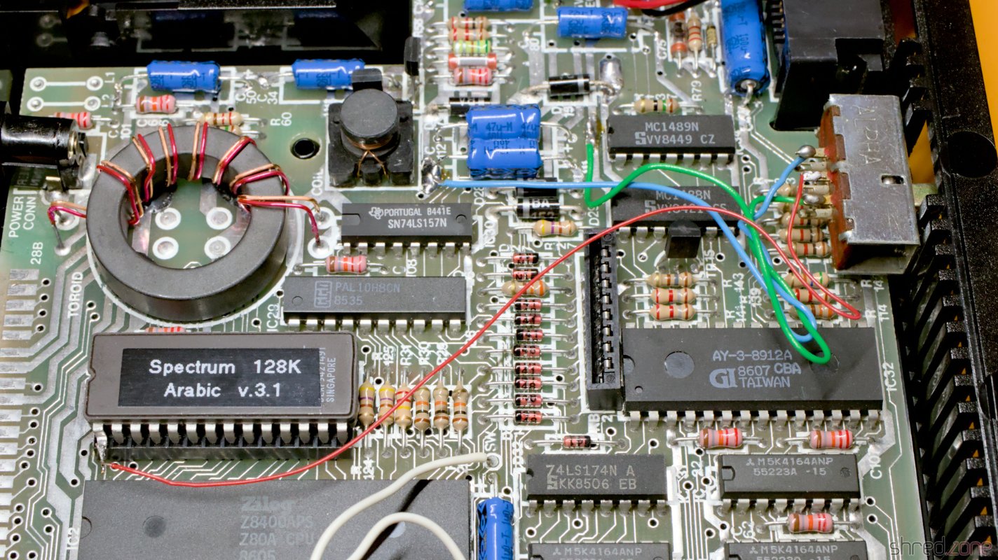
What makes this special model so curious is that it is an Arabic modification. 😀 There are stickers with Arabic letters on the keyboard, and at the front side there is a switch to select between the original 128K ROM and an Arabic version of the 48K ROM.
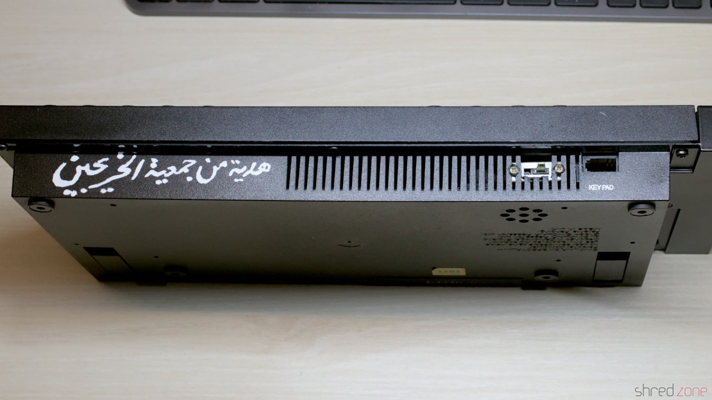
My first thought was that this was an elaborate DIY modification. But then I found a thread in a Sinclair forum. It says that Matsico, a Sinclair/Amstrad agency in Egypt, has produced these models. I could not find more information about it though, so I don't know if they were actually sold, or just made as a proof-of-concept or promotional gift.
What they all have in common, is the switch at the front, and an EPROM soldered on top of the ROM. The only known exception I found in a video by ByteDelight about a ZX Spectrum +3, where the ROM could be selected via a separate boot menu.
Restoration
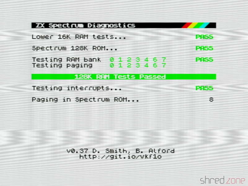
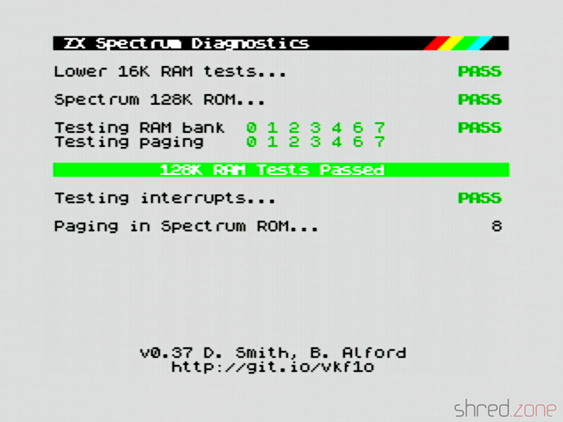
A first diagnostics run showed that the board was working fine. The only issues were massive picture interferences, and an almost inaudible sound from the AY chip.
Both issues are known problems with that model. A blog article by Adam's Vintage Computer Restorations addresses them.
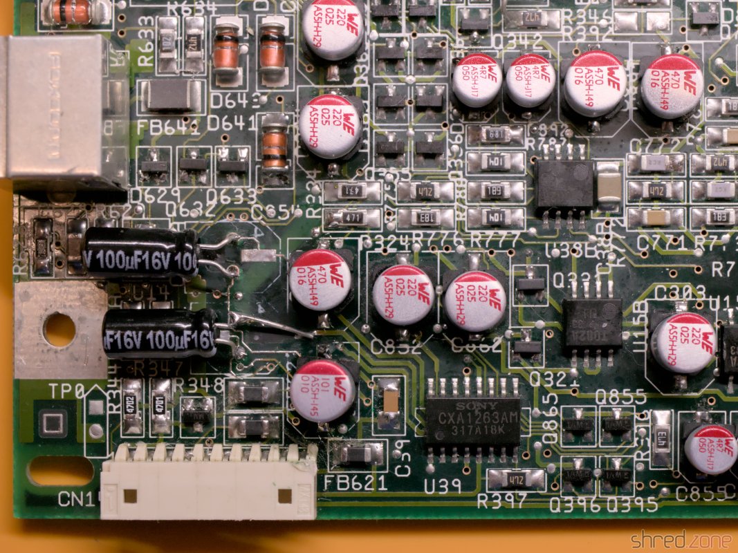
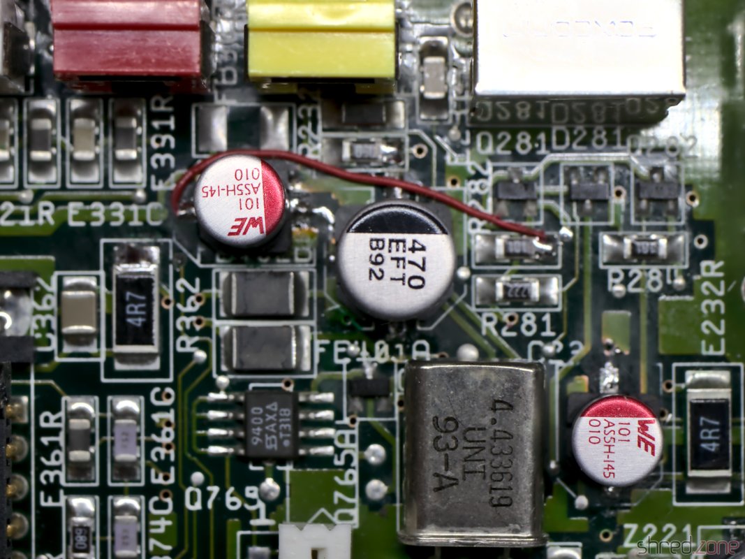
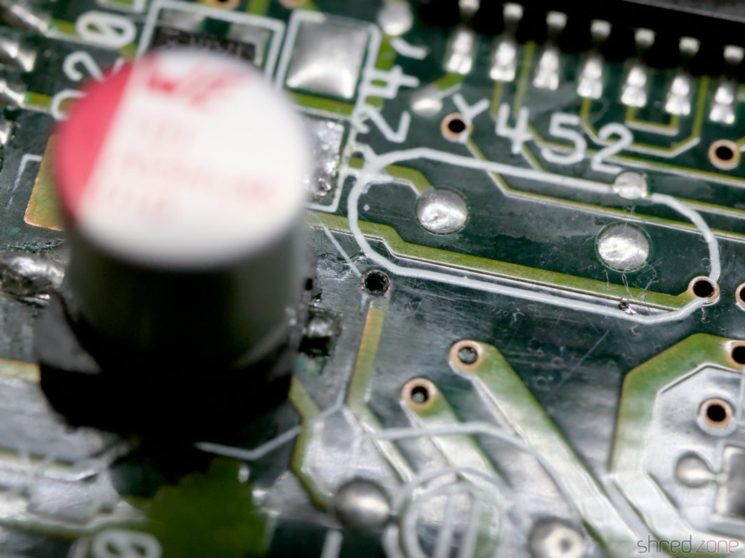
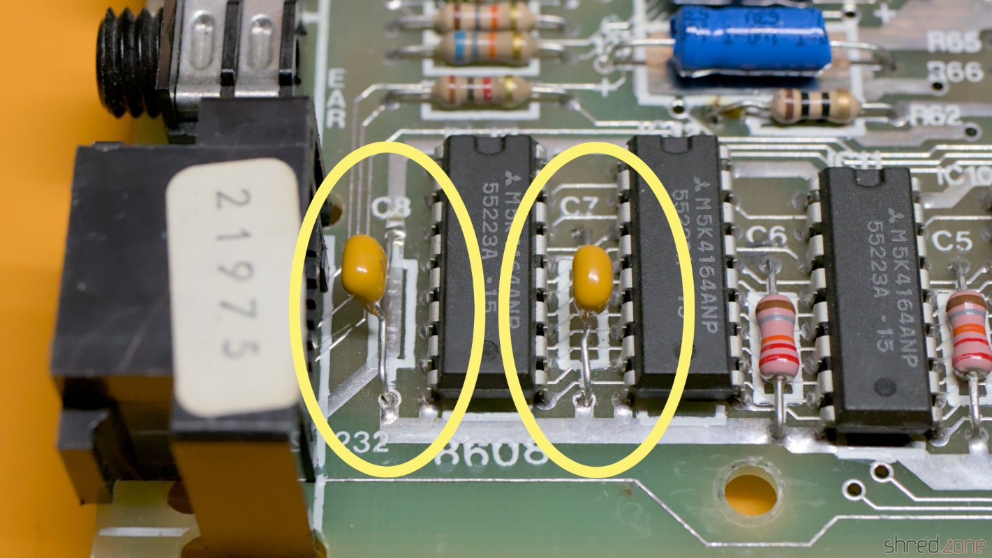
First of all, I replaced all electrolytic capacitors with premium ones. I'm doing that with all retro machines, irregarding their age and rareness. However I try my best to maintain the "retro optics", for example by using axial caps in that classic blue color.
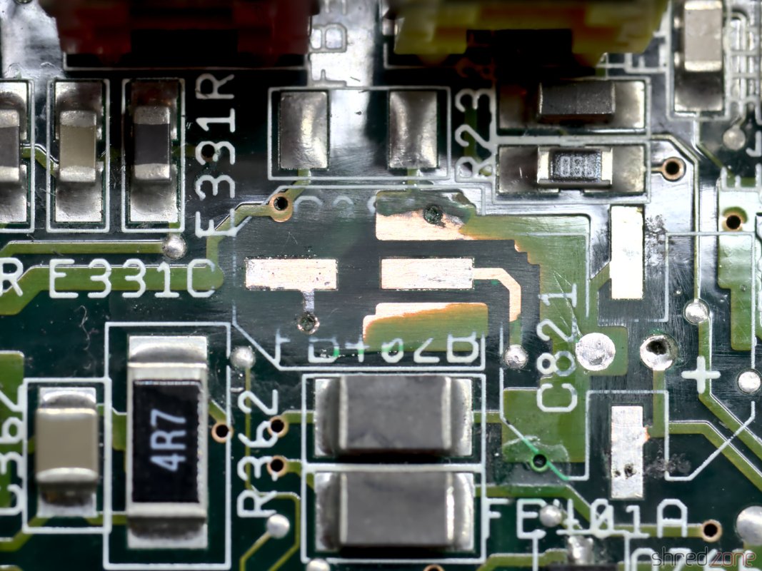
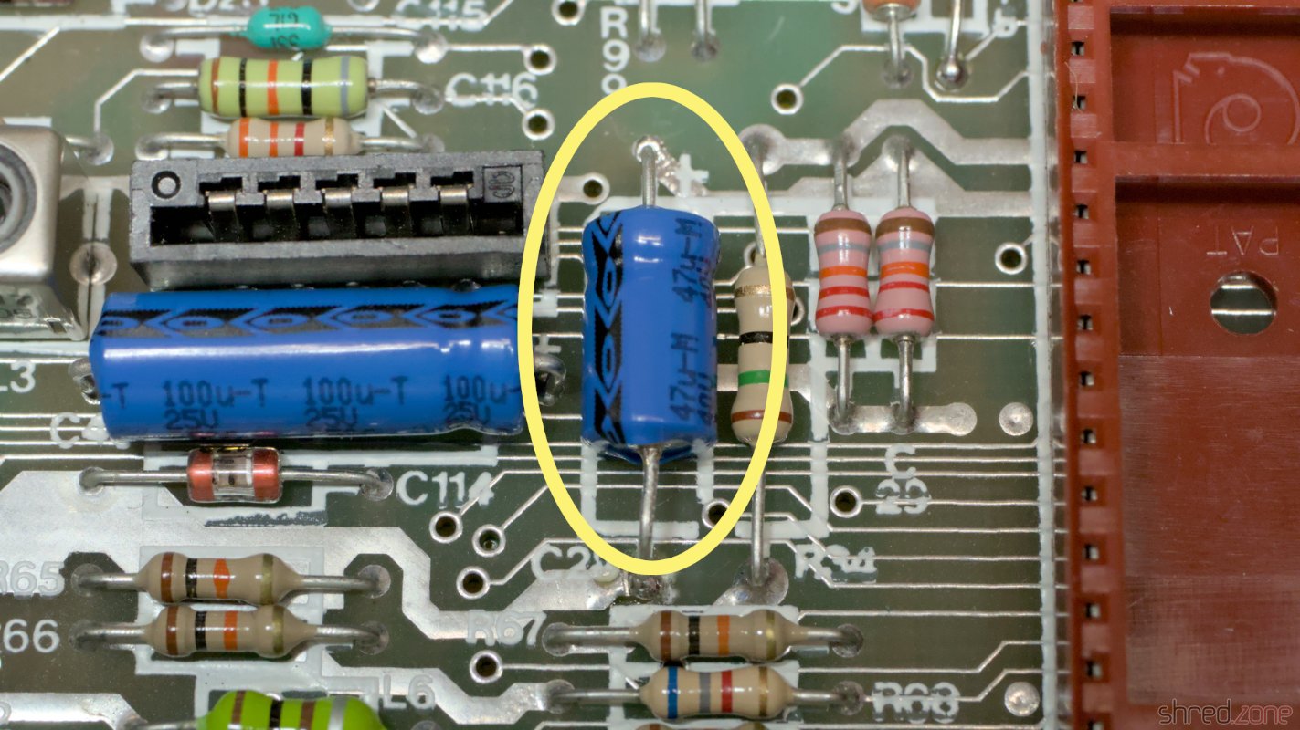
To enhance the image quality, I used a 47µF electrolytic cap for C28 (original was 22µF), and replaced C7 and C8 with 1µF MLCCs. I could also rewire C126 as mentioned in the blog article, to enhance image quality even further, but I decided to postpone that.
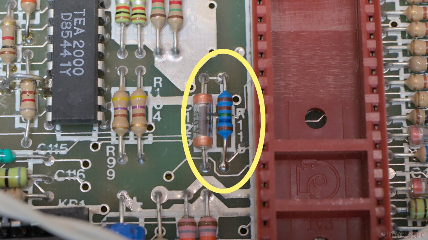
To raise the volume of the AY sound chip (so it has a similar level as the beeper), I replaced R115 with a 1.65kΩ resistor.
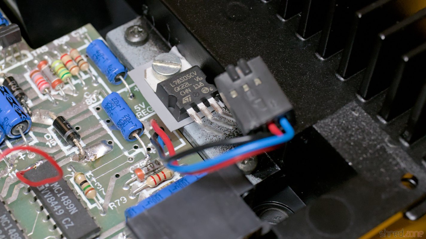
The 7805 voltage regulator is rated at 1A, and is working at its load limit on the 128K. This is the reason for the big heat sink on the right side. I replaced it with an 78S05, which is a drop-in replacement that is rated at 2A and stays considerably cooler.
I was lucky here, because in the past, someone had already replaced the 7805 with a LM1085. It is rated at 3A, but has a different pin configuration. If I had replaced it blindly, it would have killed the machine. You should always be prepared for nasty surprises when restoring old machines the previous owner already tinkered with!
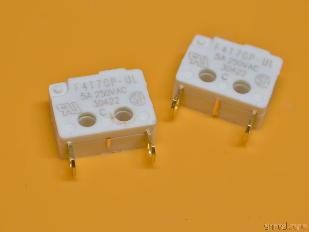
I also cleaned the case (although it was already in a very clean state). The previous owner had already replaced the keyboard membrane, but the extra keys were not working there, so I replaced it with a new membrane of a known-good brand.
The next diagnostics run showed that all tests were still green. Also the picture interferences were mostly gone (except of some minimal jailbars that I can live with), and the AY sound is much louder.
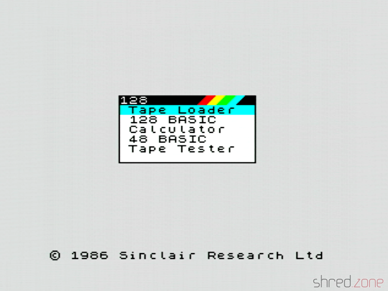
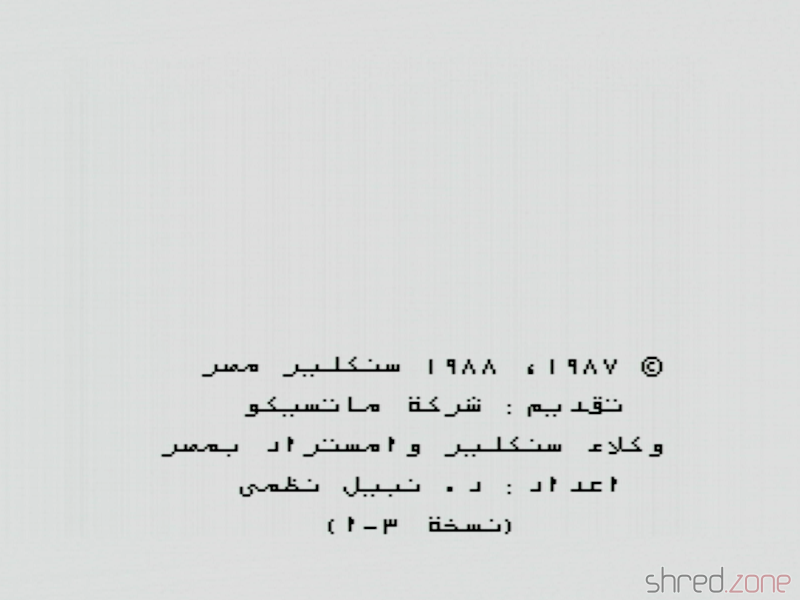
Depending on the position of the switch, the system either boots into the original ZX Spectrum 128K startup menu, or shows an Arabic boot prompt. In the Arabic version, the entire BASIC has been modified, with all texts in Arabic and written from right to left. Unfortunately I cannot read it.
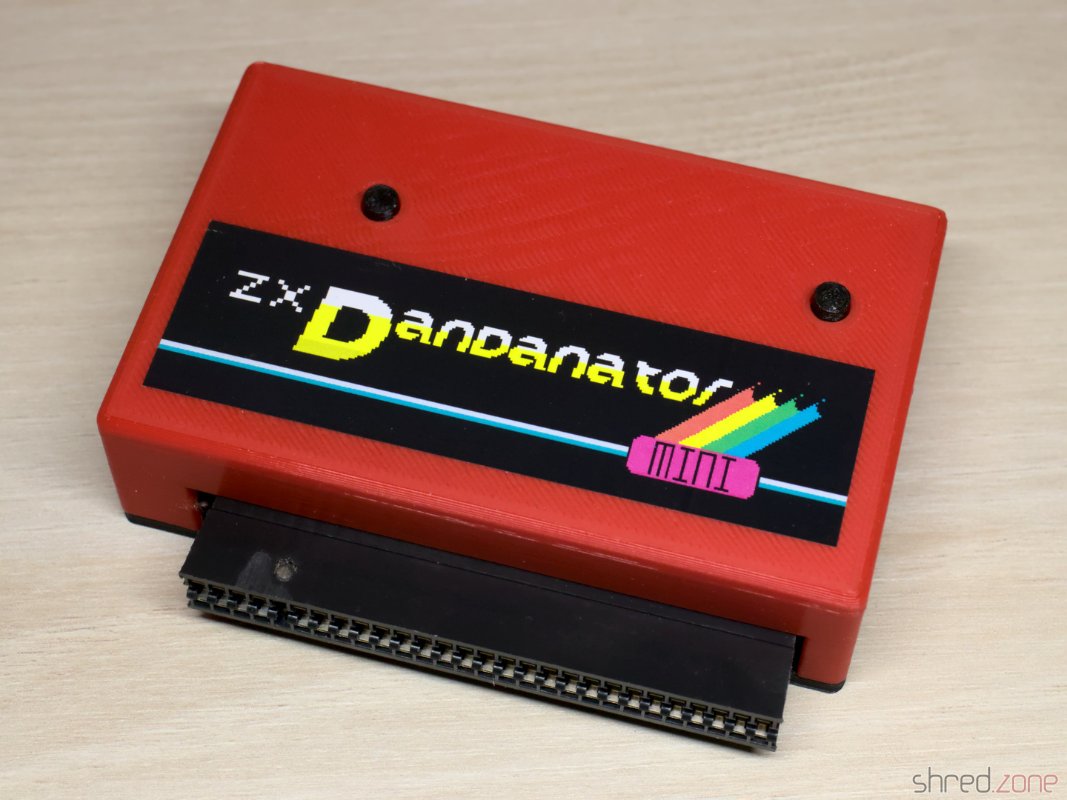
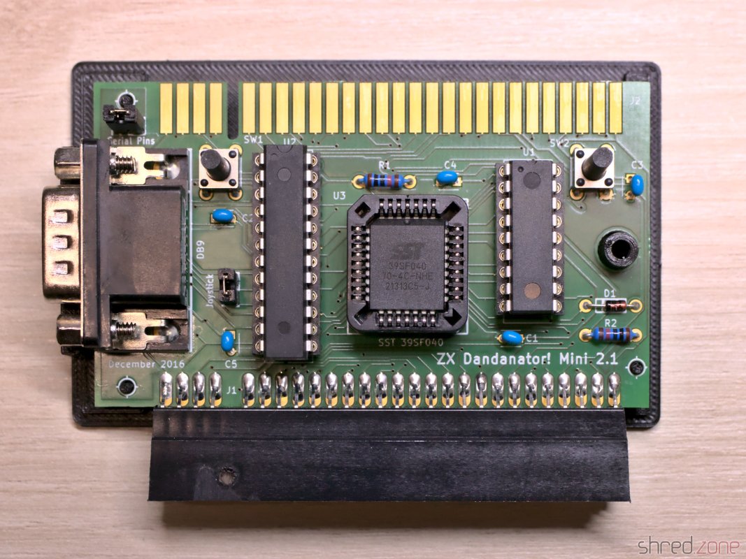
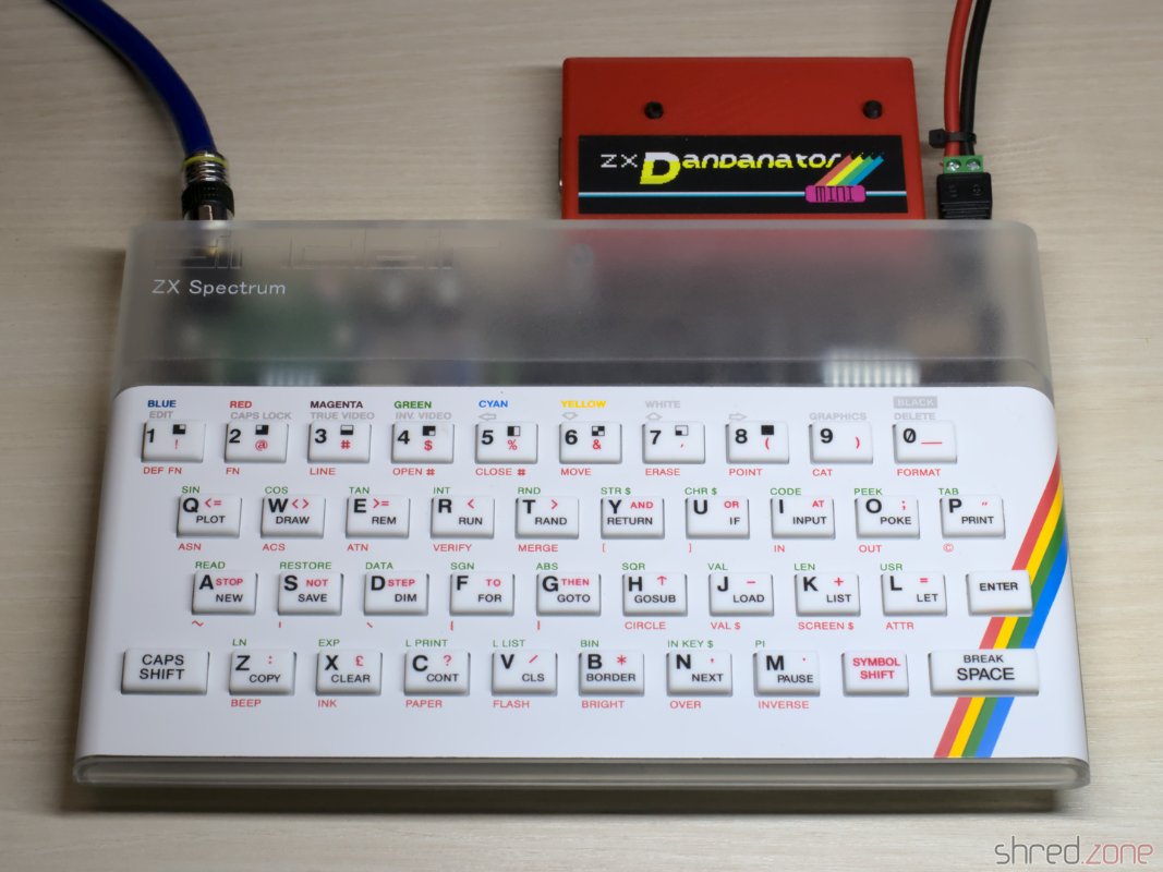
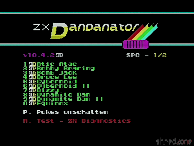
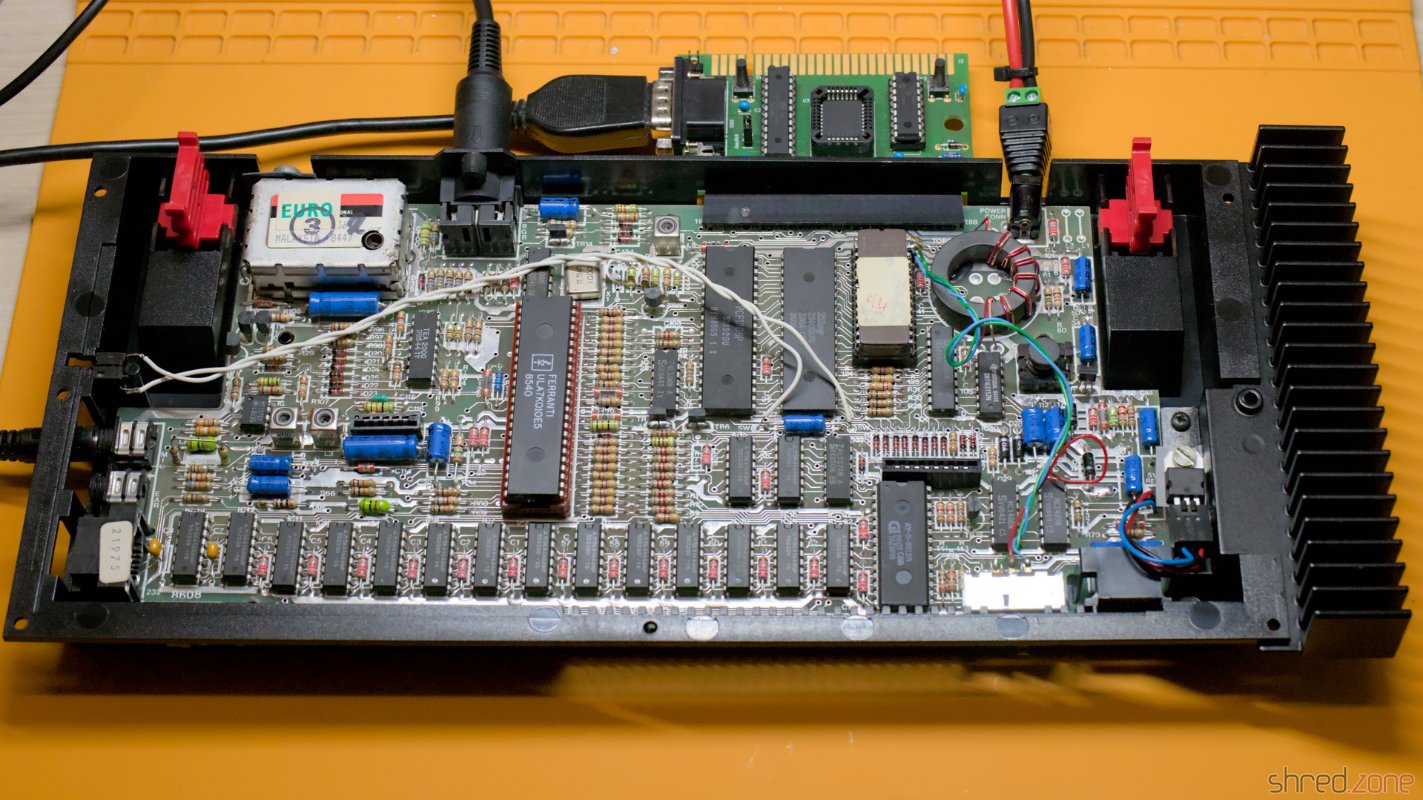
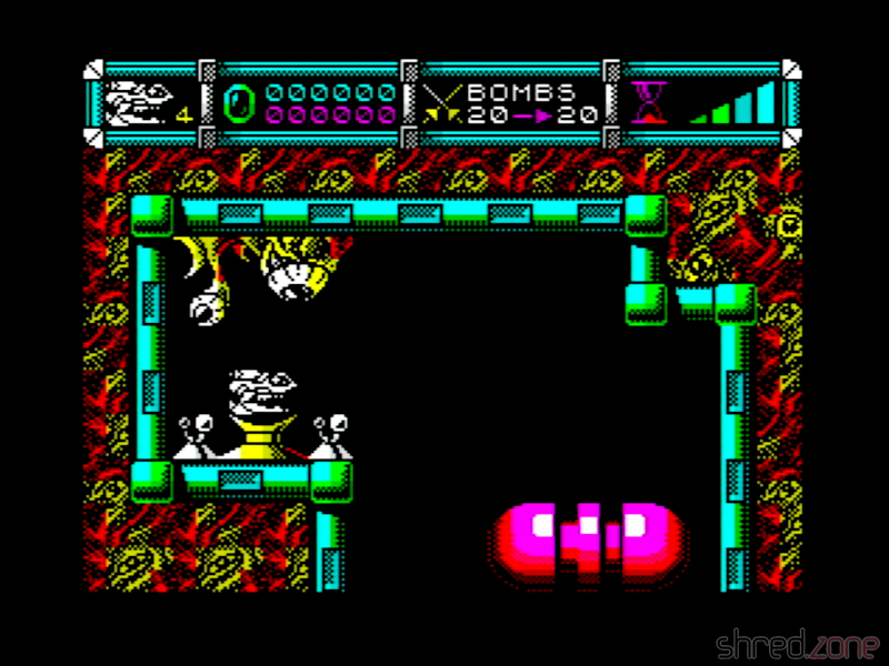
A short test with the Dandanator module also showed that games are working fine. The mandatory part of the restoration is completed!
Freestyle Restoration
There were two more things I didn't like.
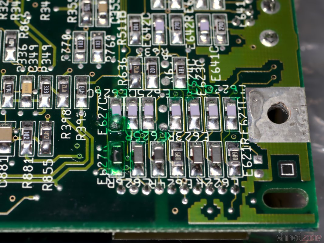
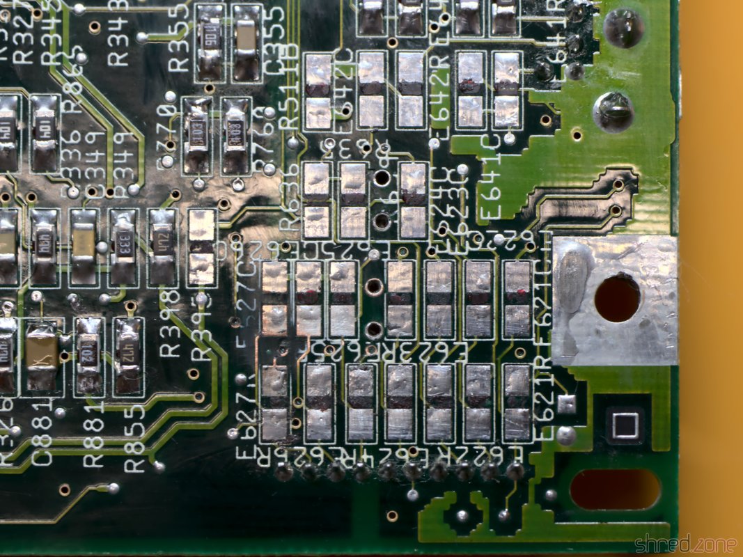
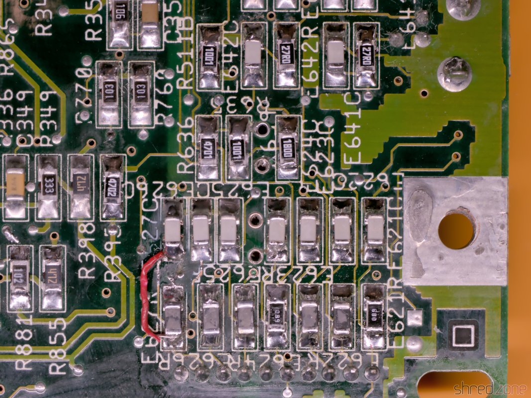
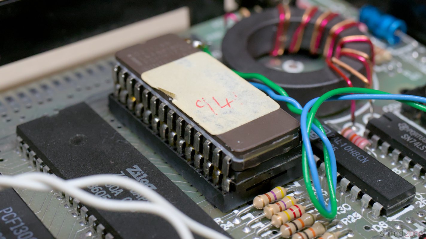
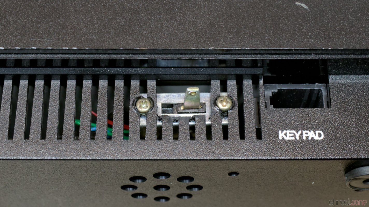
First was the ROM stack. The original solution switched the Vcc pins of the ROMs, so one of the chips was always powerless, but still connected to the address and data bus. To be honest, I wonder why this was working at all.
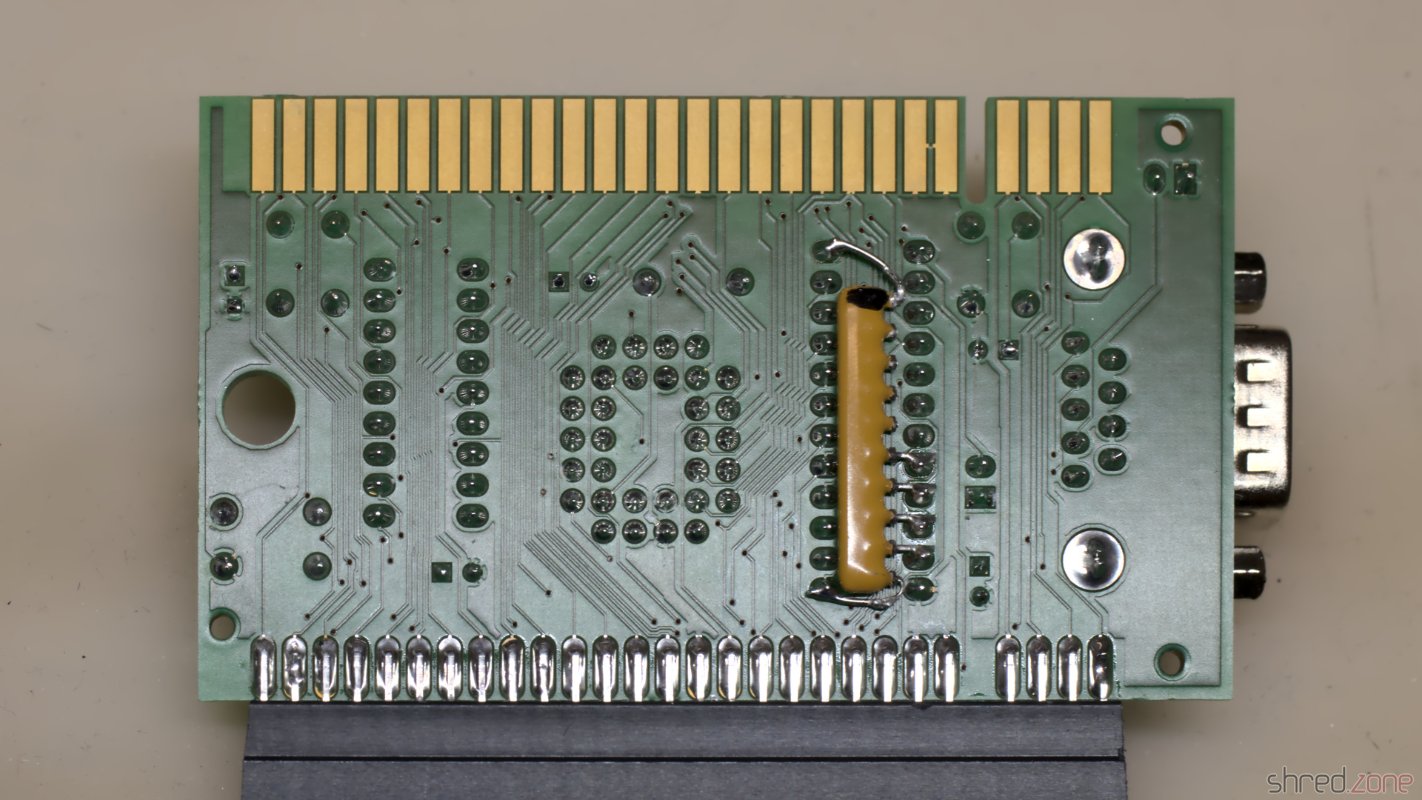
Anyway, I replaced it with a single 27C512 EPROM. On the bottom half of the memory, I burned the Arabic ROM (twice), and on the upper half, I burned the original 128K ROM. After that, I modified the switch to pull the A15 address line (pin 1) either to GND or Vcc. This way, the EPROM is always powered and the desired operating system is selected by an address line. I also upgraded the original Arabic ROM version 1 to the latest version 3.1 I could find on the web.
Of course I will keep the ROM stack. Mainly for licensing reasons, but also so that the original solution can be restored if desired.
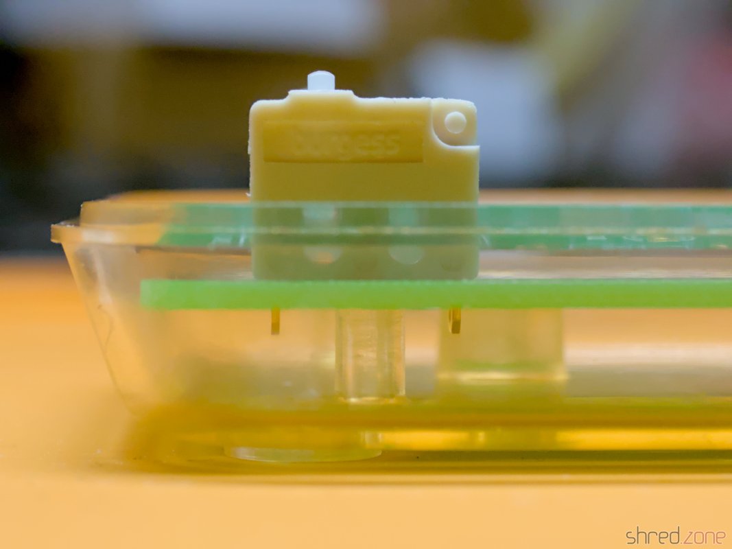
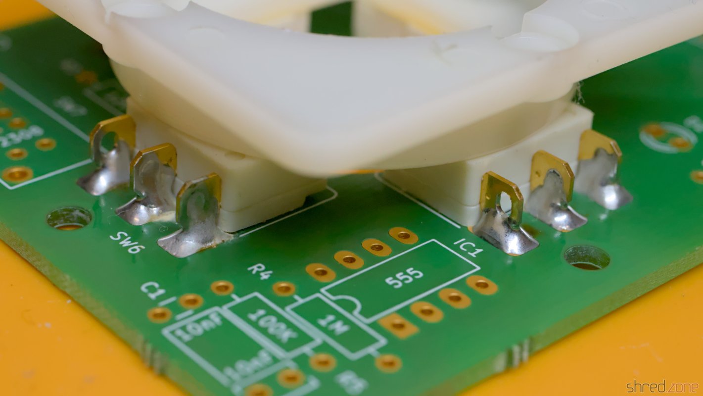
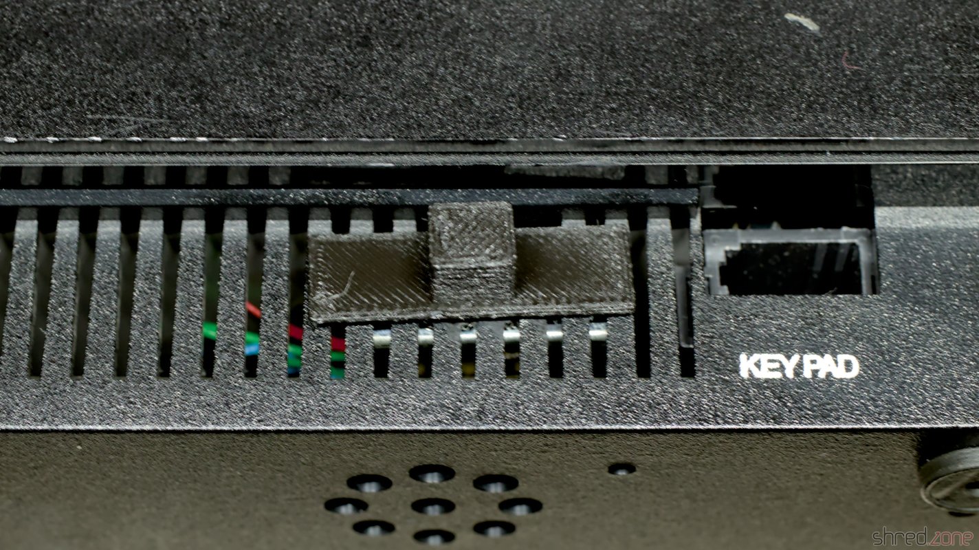
I also didn't like the optics of the naked switch at the front, so I 3D-printed a small switch cap that also covers the screws.
There are a few more things that could be done:
- I could also rewire C126 (as mentioned in Adam's blog article above), to remove the sound signal from the RGB output.
- Due to a bug in the original PAL10H8, the system crashes just by reading the $7FFD port address. There is a fix that also removes a "rain" effect caused by refresh data on the bus.
- The original ULA can be replaced with a vLA128, as a replacement if broken, or if the precious original part should be conserved.
- Dave Curran reverse engineered the numeric keypad. An ambitious tinkerer could make a DIY keypad replica.